CVD石墨烯与CVD氮化硼异质结构(4片装)
- 产地:美国
- 供应商:上海巨纳科技有限公司
- 供应商报价:面议
- 标签:CVD石墨烯与CVD氮化硼异质结构(4片装),4394,上海巨纳科技有限公司
| 品牌 | 其他品牌 | 供货周期 | 一周 |
|---|
CVD Graphene/CVD Hexagonal Boron Nitride heterostructure on SiO2/Si wafer
Properties of Graphene/h-BN Film:
Single Layer Graphene Film on Single Layer h-BN Film transferred onto 285 nm (p-doped) SiO2/Si wafer
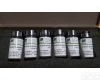
Size: 1cmx1cm; 4 pack
The thickness and quality of each film is controlled by Raman Spectroscopy
The coverage of this product is about 98%
The films are continuous, with minor holes and organic residues
High Crystalline Quality
The graphene film is premodominantly single layer (more than 95%) with occasional small multilayer islands (less than 5% bi-layers)
Sheet Resistance: 430-800 Ω/square

Properties of Silicon/Silicon Dioxide Wafers:
Oxide Thickness: 285 nm
Oxide Thickness: 285 nm
Color: Violet
Wafer thickness: 525 micron
Resistivity: 0.001-0.005 ohm-cm
Type/Dopant: P/Boron
Orientation: <100>
Front Surface: Polished
Back Surface: Etched